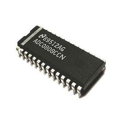
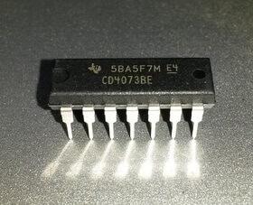
The ADC0808 data acquisition component is a monolithic CMOS device with an 8-bit analog-to-digital converter, 8-channel multiplexer and microprocessor compatible control logic. The 8-bit A/D converter uses a successive approximation as the conversion technique. The converter features a high impedance chopper stabilized comparator, a 256R voltage divider with analog switch tree and a successive approximation register. The 8-channel multiplexer can directly access any of 8-single-ended analog signals. The device eliminates the need for external zero and full-scale adjustments. Easy interfacing to microprocessors is provided by the latched and decoded multiplexer address inputs and latched TTL TRI-STATE outputs. The design of the ADC0808 has been optimized by incorporating the most desirable aspects of several A/D conversion techniques. The ADC0808 offers high speed, high accuracy, minimal temperature dependence, excellent long-term accuracy and repeatability, and consumes minimal power. These features make this device ideally suited to applications from process and machine control to consumer and automotive applications.
Where to use an ADC0808?
The ADC0808 IC is a commonly used ADC module for projects were an external ADC is required. It is a 28-pin Eight channel 8-bit ADC module. Meaning it can measure up to eight ADC value from 0V to 5V and the precision when voltage reference (Vref –pin 9) is +5V is 19.53mV (Step size). That is for every increase of 19.53mV on input side there will be an increase of 1 bit at the output side.
This IC is very Ideal to use with Microprocessors like Raspberry Pi, Beagle bone etc.. Or even to use as a standalone ADC module. Every ADC module requires a clock to function; this IC requires an external clock pulse to work. Hence, if you are looking for an ADC module with a decent resolution of 8-bit that could measure up to 8 channels then this IC is for you.
How to use ADC0808?
Since the ADC0808 IC can measure up to eight Analog voltage and also does not have an internal clock slightly requires more components to make it work compared to its predecessor ADC0804. The IC can be powered by +5V. The Vref + and the Output enable should also be supplied +5V to obtained the output. Powering the V ref + with +5V will make the IC operate with a step size of 19.53mV. The external clock should be connected to clock pin, this can either be an oscillator circuit or can just be a pulse generated from an MCU/MPU.
The right input analog voltage can be given to pins from IN1 to IN7, but the IC can read the voltage of only one channel at a time. This channel selection can be done with the pins ADD A, ADD B and ADD C. These three bits have to be set as shown in the table below to access the respective analog channel. Once the channel is set it should be enabled by making the Address latch enabled (ALE) pin to go high momentarily.

